PCB graphics with KiCad + GIMP
Update! I made a little utility to do this, as an exercise to learn some Rust.
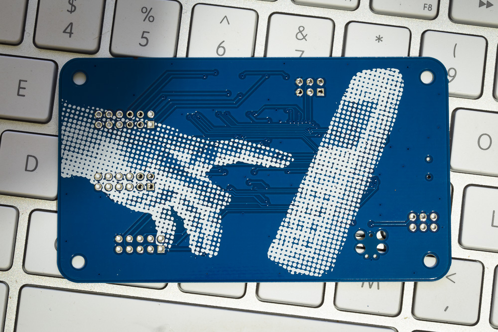
Graphics on PCBs aren’t a new thing by any stretch, but typically they’re rather geometric and simple monochromes. For a recent board, I spent a little time fiddling around with a process to create decent-looking halftone-ish PCB layers from a raster image:

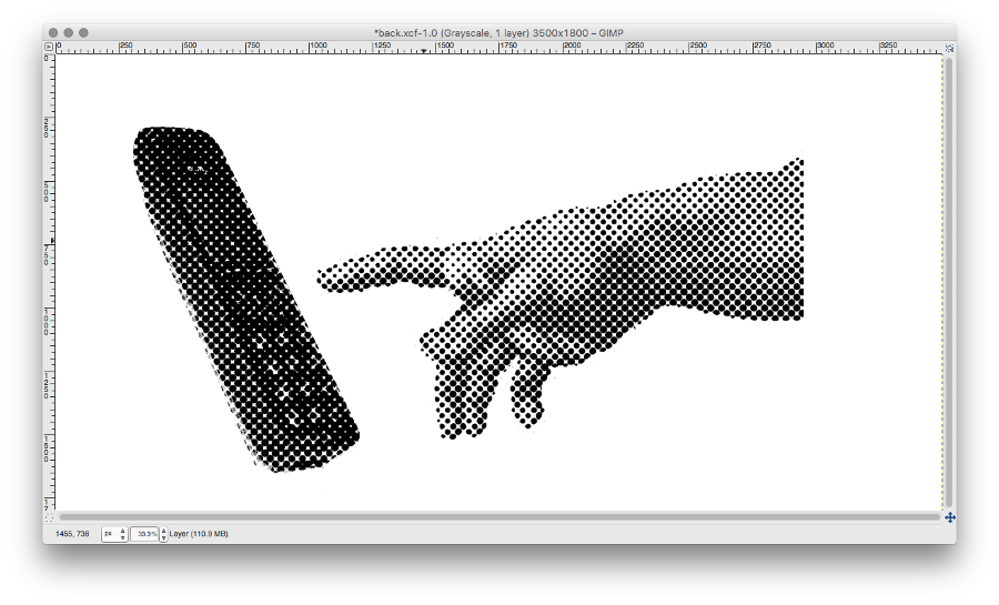
To create that, I started with a greyscale graphic in GIMP (convert it from colour by using Colors->Desaturate… then Image->Mode->Greyscale), then used Filters->Distorts->Newsprint… . There are several settings that might need adjusting in the Newsprint dialog, mainly the cell size:

I say “halftone-ish”, because when I did this, some of the original image bled through, like around the bottom-left of the phone. Nevermind, on to KiCad!
From the KiCad main launcher thingy, click the “Import Bitmap” icon:
![]()
It’s a fairly straightforward tool - first click “Load Bitmap” to bring the image in. Make sure the Pcbnew format is selected, and if you’re wanting to use an image like the above one on the silkscreen layer, tick the “Negative” box. You can view the Black&White Picture tab to preview what the resulting footprint will look like - it can be helpful when adjusting the Threshold slider. Use the Resolution boxes to control scaling of the output footprint. Export the .kicad_mod file in to a directory with name .pretty, following the normal KiCad pattern for footprint libraries.
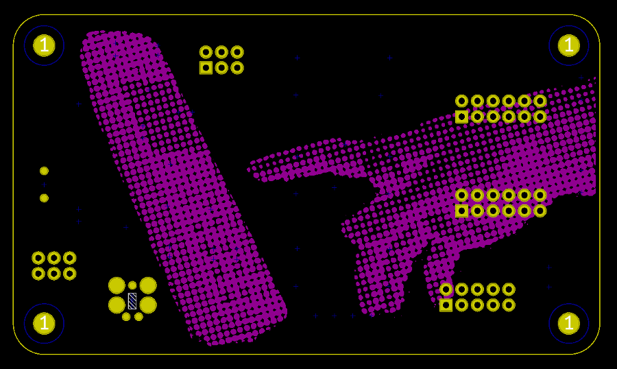
Finally, to add the footprint to a PCB, ensure the library mentioned in the previous paragraph is in your project’s path, then in Pcbnew use the “Add footprints” tool:

There’s a bit of room for improvement in this process:
First - the halftone image would ideally be a pattern of simple shapes; circles or maybe diamonds, which could be directly described in the Gerber format or .kicad_mod much more efficiently (see update at top). Using GIMP and the KiCad bitmap utility will result in a whole bunch of polygons, with some quite small. Here’s a closeup of one of the “dots” in the above footprint:

Second - I haven’t confirmed this with measurements, but it appears that the silk screening ink (which I believe is coming from a printer, not an actual silk screen, for these short-run PCBs) spreads a little bit. This means the smaller dots in particular, are physically larger than they appear in the digital file.