Making your PCB design fit with someone else's
A recent work project required designing a PCB to hold some pogo pins such that they could contact another board that I didn’t have design files for. Here’s an outline of the process that I used. I’ll call the board being designed the “jig”, and the one without design files will be the “mate”.
Ingredients
- Sacrificial mating board
- Flat bed scanner
- Raster image manipulation program, I used GIMP
- Bookkeeping tool - Python script, spreadsheet, paper & pencil, etc
- Hot air station, propane torch, or similar
- Metal spudging tool, putty knife, or similar
Procedure
There’s really not a lot to this; strip all the components off the mate so that the bare PCB will lay flat on the scanner, scan it, note the pixel coordinates of the points you’re interested in, scale and translate those coordinates to PCB coordinates for the jig.
Unfortunately, I didn’t think to get a photo of the PCB stripping process. The goal is to remove any components that would prevent the PCB from sitting flat on your scanner. Basically, I took the sacrificial mate board outside with some pliers to hold the (hot) PCB, a propane torch, spudger, sacrificial cardboard to catch components, and appropriate PPE. Use the torch to heat up the parts just until the solder starts flowing, and scrape parts off on to the cardboard using the spudger. When using a propane torch for this, it’s important to not overheat the board or it will delaminate - a normal hot air rework station would be safer, though slower.
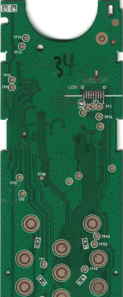
Scanning is straightforward; use the highest optical resolution setting supported by your scanner, and note down what that resolution is. Use your raster image tool to crop and orient the image properly; in my case, it was important to get the rotation just right, so the left and right edges of the board were parallel to the Y axis. This is what mine looked like:

Next, identify the points in the scanned image where you’d like to locate parts in your jig PCB design. Note down the pixel coordinates of all those points (I got those in gimp from the readout at the bottom of the image while using the picker tool), and divide by your the resolution the scan was done at. For example; a point at pixel (123, 456) in a scan done at 300DPI would be located at (10.4, 38.6)mm.
Translate those coordinates as appropriate in to your design - in my case it was easiest to start the new jig PCB design with a blank layout; first adding dowel pins, mounting clearances, and pogo pins to match up with the mating board, then designing the rest of the jig around those constraints.
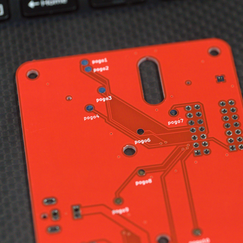
The resulting jig worked great on the first try! This was my first project using surface mount pogo pins; I’m really happy with how it went, they’re not too hard to solder, and are much easier to work with than through-hole ones for my application:
